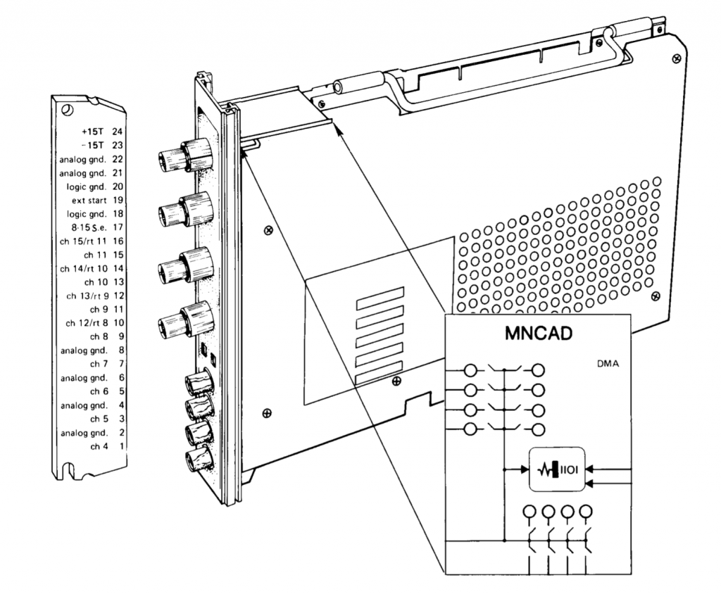
MNCAD is the A/D converter. It has 8 single-ended A/D channels on the module itself, and handles up to a total of 64 A/D single-ended and differential channels – controlling the multiplexer and pre-amplifier cards necessary.
MNCAD CSR 171000 VEC 400/404 BR 6
MNCAD has two registers; the CSR @ 171000, and BUF @ 171002. The CSR mostly follows the conventional layout – a done bit 7, an interrupt enable bit 6, a go bit 0. Unusual however is that this pattern is repeated in the high byte, and with a separate interrupt vector. The BUF register holds the result of the last conversion. There is a provision for detecting overrun; if the register is not read before a new conversion is stored, an (the?) error bit will be set.
MNCAD CSR
| 15 | err (R/W) The err bit is set when the go bit is set before the previous operation has finished (‘if go=’1′ and done=’0′ then err=’1’). It is also set when the BUF register has not been read and a new result is being stored into the BUF register (?). |
| 14 | errie (R/W) The errie bit, when set, enables interrupts when the err bit is set. The interrupt vector used will be the base vector + 4. |
| 13:8 | muxch (R/W) The channel for the next A/D operation. |
| 7 | done (R/W) Done is set when the last operation has completed. |
| 6 | ie (R/W) The ie bit, when set, enable interrupts when the done bit is set. The interrupt vector is the base vector. |
| 5 | clkovf (R/W) When set, overflow of the associated MNCKW clock module will trigger the go bit and thus start conversion. |
| 4 | ext (R/W) When set, external trigger sources are enabled to start conversion. The external trigger sources are: the ST1 on the associated MNCKW clock module. |
| 3 | enable_id (R/W) When set, the top 4 bits of the MNCAD BUF register will get the gain setting or type code of the A/D channel after the next conversion. |
| 2 | maint (R/W) When set and muxch is 0, the next conversion will be read 0 (all zeroes). When set and muxch is 1, the next conversion will be read 4095 (all ones). |
| 1 | nxc (R/O) The nxc bit is 1 when the muxch field refers to a channel that is not available. Otherwise, it is 0. |
| 0 | go (R/W) When written ‘1’, MNCAD will start a new conversion. When read ‘1’, MNCAD is busy. When ‘0’, MNCAD is idle. |
MNCAD BUF
| 15:12 | code (R/O) Zero (when ADCSR enable_id is ‘0’) or channel code for the last conversion result (when ADCSR enable_id is ‘1’) |
| 11:0 | buf (R/O) The results of the last conversion. Reading the buffer resets the ADCSR done bit. |
Information sources
The information in this page is mainly based on the VMNA listing.
Side channel
The MNCAD communicates to MNCAM (multiplexer), MNCAG (preamplifier) and MNCTP (thermocouple preamplifier) modules via a side channel. It is used to determine the configuration and the setting of front panel switches (in case of MNCAG); and also to write the programmable gain registers in MNCAG and MNCTP.
To use the side channel, software writes a value of o’77’ into the muxch register in the MNCAD CRS; followed by the desired code, and then the number of the target channel. To scan the configuration, software should program a code of o’01’ into all channels and start a conversion with the ADCSR enable_id bit set; the conversion result in ADBUF will then show the type of the channel in the bits 15:12 according to the following table:
| code | type |
| 0000 | Single ended channel (MNCAD or MNCAM) |
| 0001 | MNCTP channel |
| 0010 | Differential channel (MNCAD or MNCAM) |
| 0011 | unused |
| 0100-0111 | MNCAG, channel dial set to A |
| 1000-1011 | MNCAG, channel dial set to R |
| 1100-1111 | MNCAG, channel dial set to V |
Unknown/Missing information
From the VMNA listing, it appears to be possible to run more than one MNCAD module in a system, but it is not clear if the software would support this. Probably the only reason to have more than one module would be to speed up A/D conversions.
There is no information about the MNCTP modules; these appear to implement a gain setting register of 4 bits wide, but it is not clear what the meaning of the bits is. MNCTP seems to be of a later date than the available manuals, no description, schematics or manuals have so far been found.
Also, MNCAG is missing from the currently available schematics.
Implementation status
The current implementation is complete for the maximum of 64 single-ended channels. Software will apply a bias based on a -5.12V to +5.12V range; however, the current FPGA board A/D frontends are set up for 0V to +3.3V (DE10-Lite and DE0-Nano). The A/D frontends will implement the ‘real’ channels on the board in the lower numbered channels, and set up a multiplexer to allow the top.vhd module to insert other values into the A/D.
Other channel types besides single-ended are possible as well, but configuration for now can only be done by directly editing the sources. The interface between the MNCAD component and the A/D frontends will likely change to improve this.