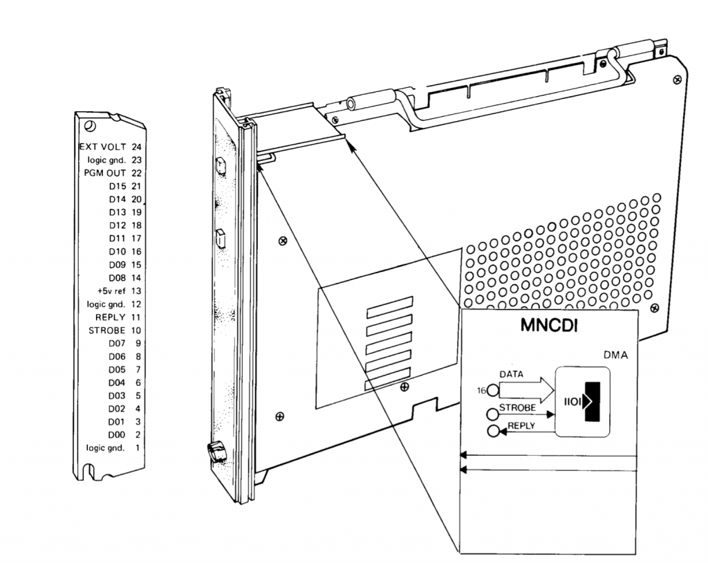
MNCDI is the Digital Input module. It allows for 16 digital input lines, plus control signals: a ‘strobe’ input, to signal that the data on the input lines is valid and should be sampled; a ‘reply’ output, to signal that the data on the input lines was successfully sampled; an ‘event’ output (on the front panel) that appears to be the same as the ‘reply’ output; and a ‘pgm out’ signal that is under software control.
MNCDI0  CSR 171160      VEC 120/124    BR 4
MNCDI1  CSR 171170      VEC 130/134    BR 4
MNCDI2  CSR 171200      VEC 140/144    BR 4
MNCDI3  CSR 171210      VEC 150/154    BR 4
MNCDI has three registers; the CSR @ 171160; the DIR (Data Input Register) @ 171162; and the SBR (Stimulus Buffer Register) @ 171164. The CSR is similar to that of most MINC modules in that it has two sets of trigger, interrupt enable bits.
The DIR has a number of interesting tricks in it. To begin, it is a write-to-zero register: when written a 1, the corresponding bit in the register will be turned off. But there is also an invert-data bit in the CSR, and that also inverts this behaviour. The top 4 bits of the DIR 15:12 can also cause a level change on each of those bits to cause the CSR done and overrun bits to set – and trigger the associated interrupt, if enabled.
The SBR Stimulus Buffer Register acts together with an enable bit in the CSR to set a mask on the DIR; if a masked bit turns on, this triggers the done and overrun bits in the CSR – again, if enabled, triggering the associated interrupt.
MNCDI CSR
| 15 | overrun (r/w) The overrun bit is associated with the 14 ‘errie’ bit and will cause an interrupt to the second vector when set. It is set on an overrun condition: when a strobe is input but the done bit in the CSR is set, signalling that the previous operation was not yet completed. It is also set when in stimulus mode (ie, the stim bit in the CSR is set) and the logical and of the SBR and the DIR is nonzero. And finally, it is set by a transition on the DIR lines 15:12 when the tren bit in the CSR is set. |
| 14 | errie (r/w) When set, an interrupt to the second vector will be triggered when the overrun bit is set. |
| 13 | unused (r/o) Will read as 0. |
| 12 | disinp (r/w) ‘disable inputs’; will disconnect the inputs from the DIR. When in maintenance mode, this will effectively cause zeros to be input to the DIR, except when the invert data bit is on, in which case ones will be input. |
| 11 | maintenance strobe (w/o) Will read as 0. Writing a one into this bit will simulate a strobe. |
| 10 | unused (r/o) Will read as 0. |
| 9 | pgmout (r/w) This bit drives the external pgmout signal; it is available for use to user programs. |
| 8 | tren (r/w) When set, level transitions on DIR inputs 15:12 cause the done and overrun bits to set, and potentially trigger the associated interrupts. |
| 7 | done (r/w) aka ‘sbr data ready’ in the schematic; apparently equivalent to the reply and event signals. The bit is set when a strobe is received and data is buffered into the DIR if in normal mode; when the logical and between the inputs and SBR is nonzero if in stimulus mode; and on level transitions on DIR inputs 15:12 when in tren mode. |
| 6 | ie (r/w) When set, enables interrupts to the first vector when the done bit is set. |
| 5 | invdata (r/w) invert data |
| 4 | pnlsw (r/w) this bit appears to defeat the front panel invert switches when set. |
| 3 | invstr (r/w) invert the strobe input |
| 2 | stim (r/w) stimulus mode; see above |
| 1 | extstrb (r/w) enable the external strobe input |
| 0 | unused (r/o) Will read as 0. |
Information sources
The workings of the MNCDI are derived from the schematics: MP00652_MNC11_Schematics_Jul78.pdf; and from the XMNB listing: AC-F419A-MC_CXMNBA0-MNCDI_Sep78.pdf
Missing information
A source that would somehow confirm the description on this page would be very helpful.
Implementation status
The implementation passes the VMNB test program without errors when set up for a loopback test or when running a logic-only test; and also it appears to work flawlessly in MINC BASIC. However, it is doubtful that the test coverage is complete, and MINC BASIC only uses the simplest functionality.