Every MINC system came with an IBV11 controller card to connect the IEEE488 (GPIB/HPIB) bus. Unlike the MNCxx modules, the IBV11 was a generic controller – you could also get it in a non-MINC system, and there was a manual documenting how to program it, as well as a maintenance print set including schematics. And even better, all of those are on Bitsavers – no need for reverse engineering! Find the manuals here: https://bitsavers.org/pdf/dec/qbus/IBV11/
In the MINC, the CSR and vectors are here:
IBV11 CSR 171420 VEC 420/424 BR 4
Note that these CSR addresses are different than the IBV11 UG mentions (16015x). The vectors are the same though.
Information sources
Besides the manuals linked above, we also used the XXDP VIBB listing and many text books on GPIB.
Missing information
None identified at the moment.
Implementation status
The latest implementation works well with MINC BASIC and the bus commands implemented by it. It has been used to interface several instruments, ranging from early-80s HP equipment using the R2D2 style, to 90s Philips/Fluke using the pre-SCPI style, to 00s Agilent using the standard SCPI style.
One open question is if parallel polling works; we have been unable so far to test because none of our test instruments supports it.
Interface hardware
It is possible to interface the FPGA directly to the bus, using only some resistors for signal conditioning and limiting the impact of transients on the FPGA. Something like a 100 ohms series resistor on each pin, a 2.2K pullup to 5V, and a 4.7K pulldown to ground. From experience with several test setups, we’ve learned that this will probably work for small setups – like, max two instruments on the bus and limited cable lengths. The interface is out of spec for the FPGA, but it will likely work even so, although we cannot rule out damage to the FPGA I/O circuits.
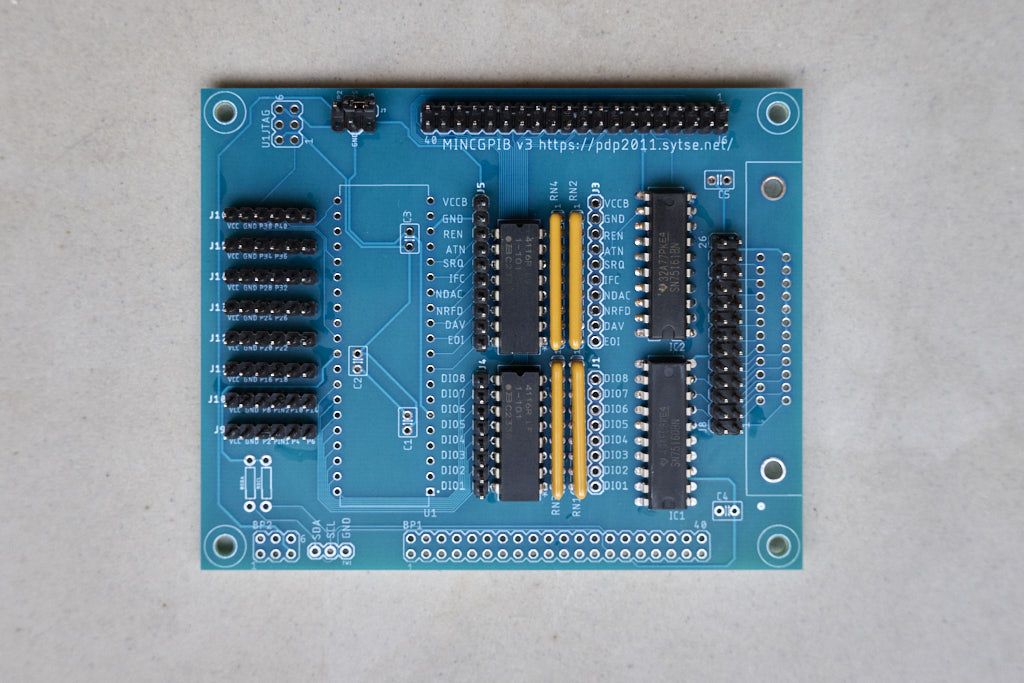
It is of course far better to use proper driver circuits, and the most obvious choice are the SN75160 and SN75161 ICs from TI. For a long time however those were not in stock with any of the usual suppliers, and TI listed the status as obsolete. But apparently that decision was reversed or at least postponed somewhat after considerable feedback from the marketplace, since TI’s website now shows the parts as being in production, and the usual places have ample stock. So I designed a PCB to interface between the Terasic-style 2×20 pin IO header and GPIB. Here it is:
Probably the most useless, unreadable schematic ever. Here’s the PCB itself:
The 40-pin connector at the top (J6) connects to the FPGA. From there, the signals go to the R1 and R2 100 Ohm DIL resistor networks – with a set of pins for connecting a logic analyzer on J4 and J5, and U1 – a 40-pin footprint for an AVR4809 with its infrastructure (C1, C2, C3, U1JTAG, RSDA, RSCI, TWI, BP1, BP2), but please ignore all that, because at the moment there’s nothing more than a vague outline of a plan for the AVR, and it might never happen.
To the right of the R1 and R2 DIL resistor arrays, there are the RN3 and RN4 2.2k pullup resnets, and the RN1 and RN2 4k7 pulldown resnets. Right of those, you’ll see another pair of logic analyzer connections J1 and J3. Then the real business about the board: IC1 and IC2, the SN75160 and SN75161.
At the edge of the board, you’ll see a 2×13 pin header, and the outline of a GPIB connector. You could install the GPIB connector there, but my current recommendation is that you install the 2×13, and use a 2×13 flatcable to connect to the ‘mincplug’ bulkhead connector PCB I designed – even if you don’t have a bulkhead in mind, it’ll help to keep the FPGA and interface boards from being dragged around by the heavy GPIB cables. And also, if you don’t have real GPIB cables handy, you can use the flat cable to reach your instrument, and also you can probably get away with linking the ‘plug’ boards with 2×13 flatcable to connect more than one – that’s why there are 2 2×13 header footprints on the plug PCB.
Back to the mincgpib board, in the top left corner between the 2×3 U1JTAG and the 2×20 J6, you’ll see a T-shaped connector labelled J7 (and J17). Sorry, the print is small, I’m still learning PCB design. That header is for the power supply to the GPIB components – the pullups and the driver ICs IC1 and IC2. You can choose to use the 5V from the FPGA connector; in that case, connect the pins labeled BUS and J6. Or you can use an external (lab) power supply; connect that to BUS and GND, or J17. The BP2 pin is for future plans – please don’t use that until I’m finished with the MINC backplane design.
Finally on the left edge you’ll see a row of 1×6 pin headers J9 through J15. Those bring out the FPGA I/O pins on the 2×20 that are not used for the GPIB interface. J9 and J10 are laid out for the PMOD SPI standard – note that the pins 4, carrying the PIN1 and PIN2 signals might be input-only depending on your FPGA board. J11 through J15 are laid out for the PMOD I2C standard, so there are only 2 data signals for each connector.
The topmost 1×6, J16, pin 40 is used for the TE talk enable signal towards the SN7516x drivers, and pin 38 is reserved for logic analyzer connection.
All the 1×6 headers from J9 through J16 are at .200 spacing – put them in a female header at a 90 angle to keep them straight, it makes for easy soldering and a much nicer board.
The following table gives the mapping between the pins on the 2×20 header, the signal names in the schematic and the corresponding GPIB signal names, and the pins that they map to on the FPGA. For these boards you can also find those already defined in the appropriate board directory QSF file.
| Pin # | Name in schematic | GPIB signal | DE10-Lite pin | DE0-Nano pin |
|---|---|---|---|---|
| 1 | PIN1 | – | PIN_V10 | |
| 2 | P2 | – | PIN_W11 | |
| 3 | PIN3 | – | PIN_V9 | |
| 4 | P4 | – | PIN_W9 | |
| 5 | PD6 | ATN | PIN_V8 | |
| 6 | P6 | – | PIN_W8 | |
| 7 | PD5 | SRQ | PIN_V7 | |
| 8 | P8 | – | PIN_W7 | |
| 9 | PD7 | REN | PIN_W6 | |
| 10 | P10 | – | PIN_V5 | |
| 11 | VCC5 | – | – | |
| 12 | GND | – | – | |
| 13 | PA0 | DIO1 | PIN_W5 | |
| 14 | P14 | – | PIN_AA15 | |
| 15 | PA1 | DIO2 | PIN_AA14 | |
| 16 | P16 | – | PIN_W13 | |
| 17 | PA2 | DIO3 | PIN_W12 | |
| 18 | P18 | – | PIN_AB13 | |
| 19 | PA3 | DIO4 | PIN_AB12 | |
| 20 | P20 | – | PIN_Y11 | |
| 21 | PA4 | DIO5 | PIN_AB11 | |
| 22 | P22 | – | PIN_W11 | |
| 23 | PA5 | DIO6 | PIN_AB10 | |
| 24 | P24 | – | PIN_AA10 | |
| 25 | PA6 | DIO7 | PIN_AA9 | |
| 26 | P26 | – | PIN_Y8 | |
| 27 | PA7 | DIO8 | PIN_AA8 | |
| 28 | P28 | – | PIN_Y7 | |
| 29 | VCC33 | – | – | |
| 30 | GND | – | – | |
| 31 | PD0 | EOI | PIN_AA7 | |
| 32 | P32 | – | PIN_Y6 | |
| 33 | PD1 | DAV | PIN_AA6 | |
| 34 | P34 | – | PIN_Y5 | |
| 35 | PD2 | NRFD | PIN_AA5 | |
| 36 | P36 | – | PIN_Y4 | |
| 37 | PD3 | NDAC | PIN_AB3 | |
| 38 | P38 | – | PIN_Y3 | |
| 39 | PD4 | IFC | PIN_AB2 | |
| 40 | TE | TALK ENABLE | PIN_AA2 |
Bill of Material
The following components are needed for the mincgpib and mincplug PCBs:
| Ref designation | Component | Desc |
|---|---|---|
| IC1 | TI SN75160BN | Driver, DIO1:8 |
| IC2 | TI SN75161BN | Driver, GPIB Control |
| R1, R2 | BOURNS 4116R-1-101LF | RES ARRAY 8RES 100Ohm 16DIP |
| RN1, RN2 | BOURNS 4609X-AP1-472LF | RESNET 8RES 4k7 9SIP |
| RN3, RN4 | BOURNS 4609X-AP1-222LF | RESNET 8RES 2k2 9SIP |
| J2 | NORCOMP 112-024-113R001 | SCSI PLUG 24POS R/A SOLDER |
| J6 | 2×20 | |
| J8 | 2×13 | (or 2 for a mincplug setup) |
| J7 | 2×3 | pull out 2 pins, or use 1×2 for j6-bus |
| J9-J16 | 1×6 | optional, for other MINC I/O |
| J1,J3 | 1×8 | optional, logic analyzer |
| J4,J5 | 1×10 | optional, logic analyzer |
This is what a finished board would look like – note that I’ve added the optional J4 and J5, and that the board is set up for using the gpibplug bulkhead connector. Also note J7 with a jumper on the top right two pins (hardly visible in the photo), to select power from the FPGA 5V pin: